Scanning Electron Microscope

How it works
Scanning Electron Microscope (SEM): a type of electron microscope that permits the observation and characterization of heterogeneous organic and inorganic materials on a nanometre (nm) to micrometre (μm) scale. The SEM is capable of obtaining 3D-like images of the surfaces of a very wide range of materials. The surface area to be examined or the micro-volume to be analysed is irradiated with a finely focused electron beam, which may be swept in a raster across the surface of the specimen to form images or may be static to obtain analyses at one point. Signals produced from the interaction of the electron beam with the sample are in the form of secondary electrons (emitted from the sample), backscattered electrons (from the impinging electron beam) or characteristic X-rays. Signals are obtained from specific emission volumes within the sample and can be used to examine many characteristics of the sample (surface topography, crystallography, chemical composition, etc.).
Research topics include the investigation of the morphology and thickness of various semiconductor or insulator films obtained through atomic layer deposition techniques, as well as diatoms or diatomaceous algae (both freshwater and marine), desert dust, microplastics, bacteria, orthodontic samples, aerosols, and many other materials.
Our device
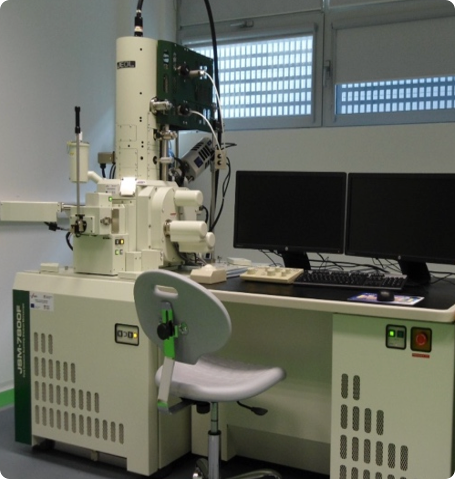
JEOL Field Emission Scanning Electron Microscope (JSM-7800F) with maximal resolution of 0.8 nm, acceleration voltage of 0.01 – 30 kV and the magnification range: x25 – x1000000, equipped with the following detectors:
- Lower secondary electron detector (LED)
- Upper secondary electron detector (UED)
- Backscattered electron detector (BED)
- Scanning Transmission Electron Microscopy (STEM) detector
- Energy dispersive X-ray spectrometer X-MaxN 80, Oxford Instruments (EDS) – used for the analysis of the elemental composition of the specimen
Our sample preparation devices
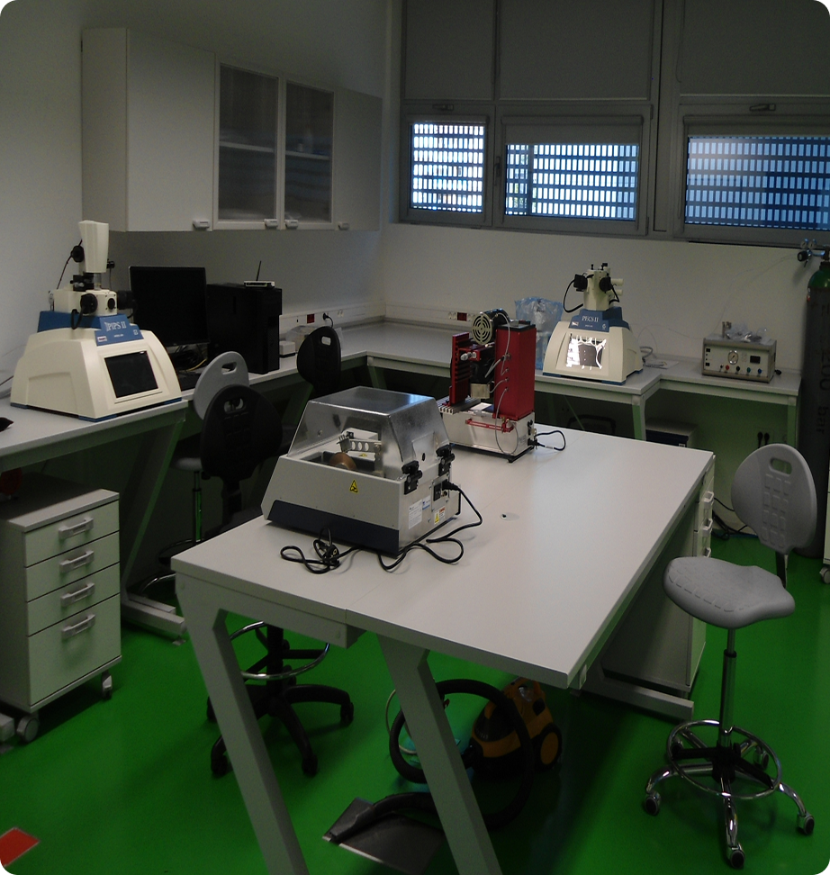
Various precision devices for sample preparation
- Precision Etching and Coating System (Gatan PECS II Model 685) – with two ion guns for etching solid samples with low-energy Ar+ ions (energy range 0.1 – 8 keV). It can also be used for coating samples with C, Au, Pt/Pd, Cr, and Pt.
- Precision Ion Polishing System (Gatan PIPS II Model 695) – with two ion guns for polishing solid samples with low-energy Ar+ ions (energy range 0.1 – 8 keV). Primarily used for sample preparation for scanning transmission electron microscopy (STEM).
- Critical Point Dryer (Quorum K 850) – used for dehydration of biological samples (replaces water with liquid CO2).
- Precision Diamond Wire Saw (Well 3242) – stainless steel wire with diamond particles used for cutting various types of samples. It provides smooth and sharp edges.
- Disc Grinder – used for thinning samples.
- Dimple Grinder – used for thinning samples to electron transparency suitable for STEM/TEM analysis.
- Contact:
- Assoc. Prof. Ivna Kavre Piltaver, PhD
- ivna.kavre@uniri.hr
- +385 51 584 618
- Contact:
- Assoc. Prof. Ivna Kavre Piltaver, PhD
- ivna.kavre@uniri.hr
- +385 51 584 618
X-ray Photoelectron
Spectroscopy

How it works
X-ray Photoelectron Spectroscopy (X-ray Photoelectron Spectroscopy, XPS), also referred to as Electron Spectroscopy for Chemical Analysis (Electron Spectroscopy for Chemical Analysis, ESCA), irradiates the sample surface with a soft (low energy) X-ray. This X-ray excite the electrons of the sample atoms and if their binding energy is lower than the X-ray energy, they will be emitted from the parent atom as a photoelectron. Only the photoelectrons at the extreme outer surface (10-100 Å) can escape the sample surface, making this a surface analysis technique. XPS analysis not only provides elemental information, but because the technique is detecting the binding energy of emitted electrons, it can also provide some chemical bonding information. Depending on what elements the parent atom is bound to, the binding energy of the emitted photoelectrons may shift slightly. The instrument is sensitive enough to detect these electron energy shifts and use them to determine what chemical compounds are present. The XPS spectrometer is also equipped with an ion gun which allows depth profiling of the sample surface. This is extremely useful in determining if contaminants are only present on the surface or reside in the sample bulk.
Our device
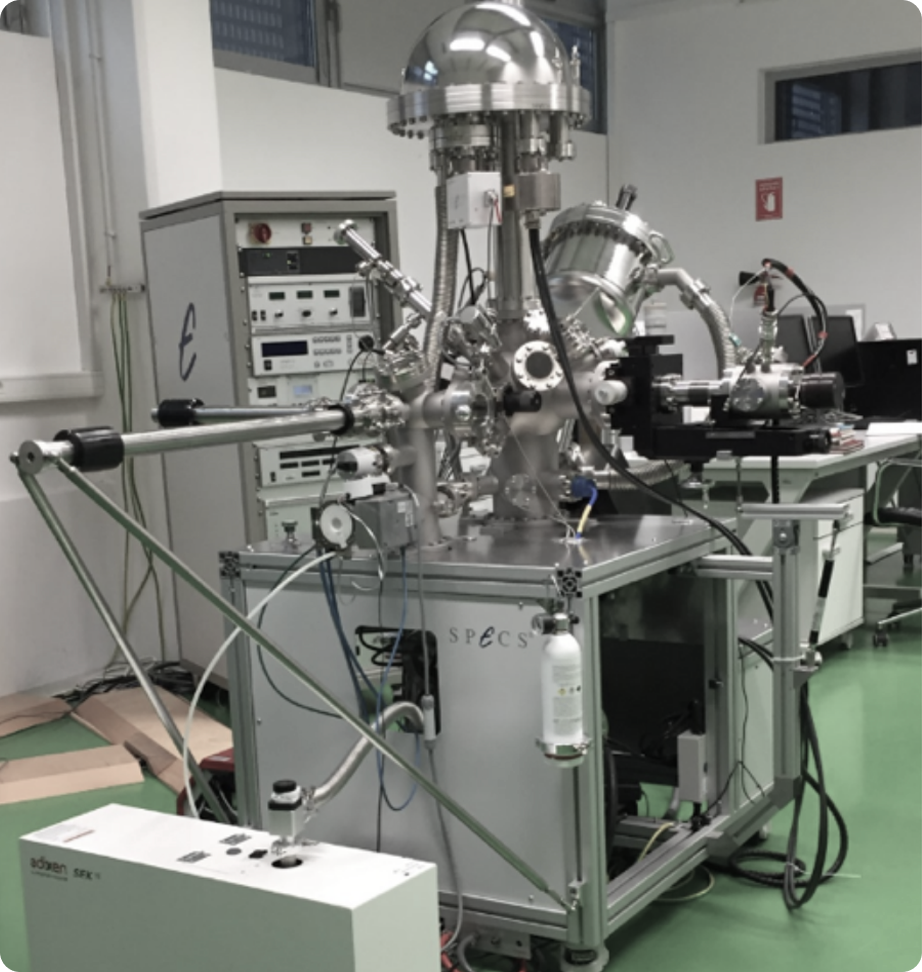
XPS is a SPECS system equipped with the following additional devices:
- FOCUS 500 – X-ray source
- PHOIBOS 100 MCD-5 – 100 mm hemispherical analyzer
- IQE 11/35 – ion gun for low-energy ions of inert and reactive gases (0.3-5 keV)
- LN2 - 800oC – precise XYZ manipulator samples holder with controlled heating and cooling
- turbo pump (Pfeiffer) and titanium sublimation pump (Hositrad) for the main chamber, turbo pump (Pfeiffer) for prechamber
- sealed water-cooling system for the X-ray source and vacuum turbo pumps
- FG 500 – electron gun
- Contact:
- Assoc. Prof. Robert Peter, PhD
- rpeter@phy.uniri.hr
- +385 51 584 621
- Contact:
- Assoc. Prof. Robert Peter, PhD
- rpeter@phy.uniri.hr
- +385 51 584 621
Secondary Ion Mass Spectrometry

How it works
Secondary Mass Ion Spectrometry (Secondary Ion Mass SpectrometrySIMS) is a microanalytical technique used to understand the composition (isotopic, elemental, and/or molecular) of any predefined microvolume from solid material. This technique is particularly useful in semiconductor research and technology for measuring the concentrations of the impurities in the materials. Detection limits for most of the elements are in the ppm or ppb range, making SIMS one of the most sensitive methods for the elemental analysis. SIMS derives compositional information by directing a focused energetic ion beam at the surface of interest. These ions, referred to as primary ions, induce the emission of atoms and molecules from the solid’s surface, a small percentage of which exist in the ionized state. The emitted ions, referred to as secondary ions, are then collected and passed through a mass spectrometer.+, O2+ ili Ar+, a može detektirati pozitivne ili negativne sekundarne ione (atomske i molekularne) u rasponu od 1 amu do 500 amu, koristeći kvadrupolni maseni analizator.
SIMS measurements can be performed in three operating modes: Static SIMS: measurement of mass spectra of the specimen surface; Dynamic SIMS: depth profiling of selected elements or molecules in the sample; Surface imaging: elemental imaging of the sample surface.
Our device
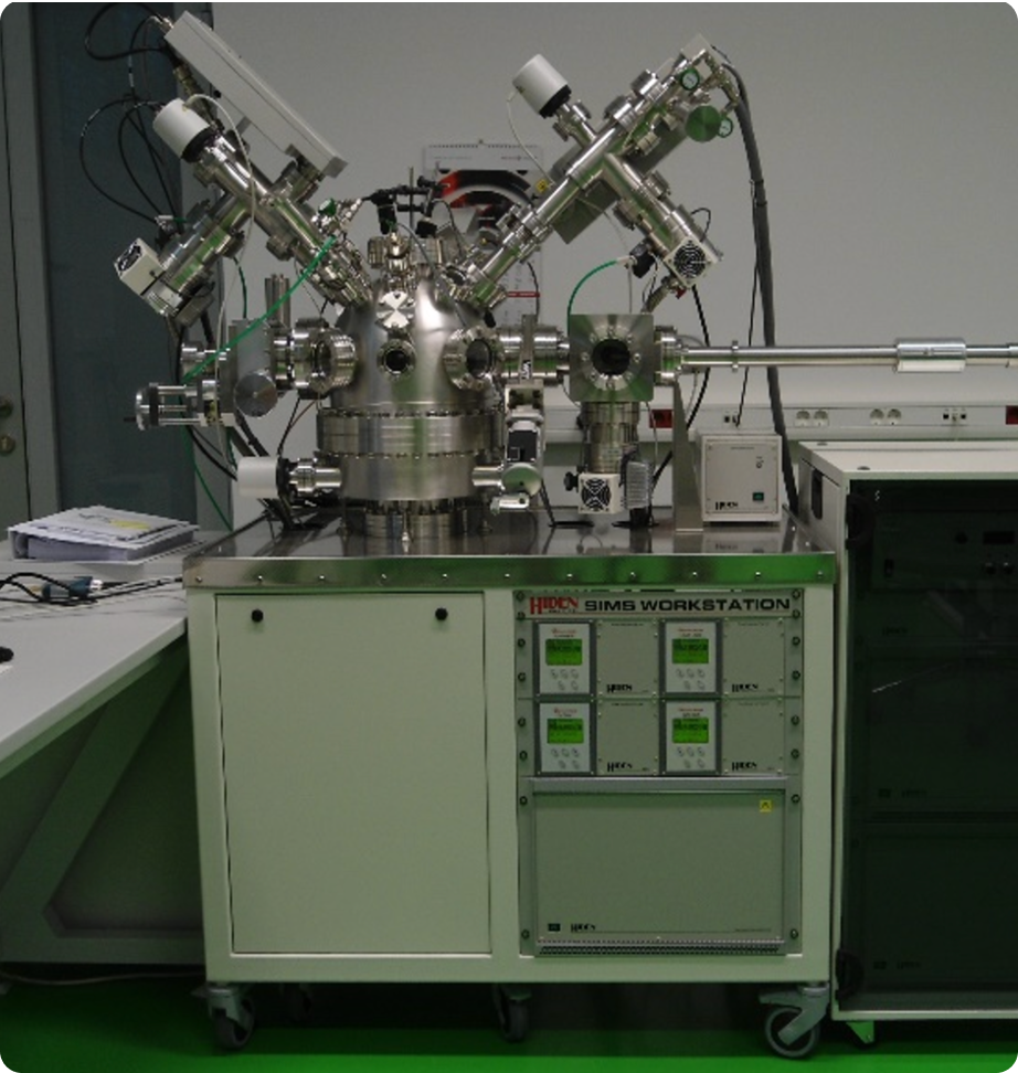
SIMS instrument is a Hidden system with the following equipment:
- ion gun for low-energy ions of inert and reactive gases (IG20) with energy range of 0.5 – 5 keV (O2+ or Ar+ ions) and ion-beam diameter of 100 μm
- Caesium ion gun (IG5C) with energy range of 0.5 – 5 keV and ion-beam diameter of 100 μm
- quadrupole mass analyser (MAXIM HAL7) with mass range: 1 – 500 amu and Puls Ion Counting Electron Multiplier detector
- ionization source for Residual Gas Analyser (RGA)/Sputtered Neutral Mass Spectrometry (SNMS) mode
- electron gun (FG 500 – SPECS system) – for the neutralization of surface charging effects
Our sample processing device
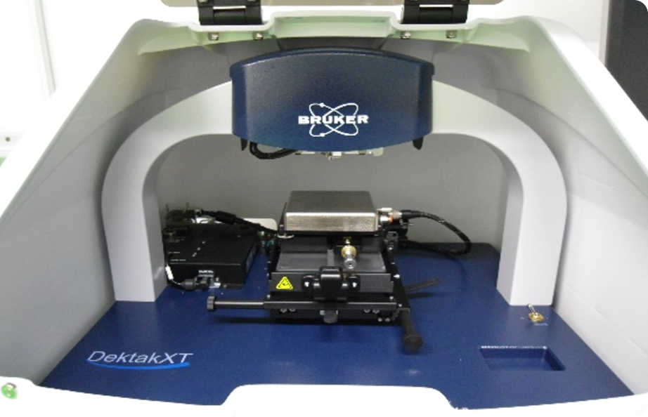
Bruker DektakXTTM stylus profiler is used for measuring various physical properties of the surface of the material. In our laboratory, it is primarily used for measuring the crater depth after SIMS depth profiling and the surface roughness.
- Contact:
- Assoc. Prof. Robert Peter, PhD
- rpeter@phy.uniri.hr
- +385 51 584 621
- Contact:
- Assoc. Prof. Robert Peter, PhD
- rpeter@phy.uniri.hr
- +385 51 584 621
Atomic Layer Deposition

How it works
Atomic Layer Deposition (ALD) is a technique used for a deposition of thin inorganic films, characterized with an excellent precision of thickness of deposited films (in Å-nm range). ALD can be used to coat wafers, planar objects and porous bulk materials, as well as particles and complex 3D objects. The essence of this technique is to alternately expose surface of the substrate to two different gas compounds (precursors), and this process is repeated in a cyclic manner. The self-limiting aspect of ALD leads to excellent step coverage and conformal deposition, i.e. the deposited film is homogeneous and non-porous. Most synthesized materials in our ALD system are semiconductor or isolating thin films such as oxides: ZnO, Al2O3, TiO2, SiO2 and nitrides: AlN, TiN, Si3N4.2O3, TiO2, SiO2 i nitridi: AlN, TiN, Si3N4.
Our device
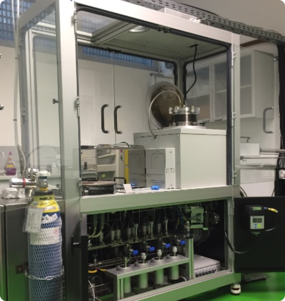
Our Atomic Layer Deposition (ALD) instrument is a Beneq TFS 200 system
- Substrate temperature range: 25 - 500 °C
- Maximal substrate dimensions (regular chamber): 200 mm in diameter, 3 mm in height
- Maximal substrate dimensions for 3D chamber: 200 mm in diameter, 95 mm in height
- Capacitive coupled plasma system (operates at RF of 13,6 MHz and plasma power up to 300 W)
- Ozone generator (ozone can be used as an oxygen source for ALD synthesis)
- 4 liquid sources attached to the instrument.
- Contact:
- Assoc. Prof. Iva Šarić Janković, PhD
- iva.saric@uniri.hr
- +385 51 584638
- Contact:
- Assoc. Prof. Iva Šarić Janković, PhD
- iva.saric@uniri.hr
- +385 51 584638
Spectrophotometer

How it works
The UV-Vis spectrophotometer enables spectrophotometric measurements in the ultraviolet and visible parts of the spectrum.
In our laboratory, we frequently investigate the decolorization of dyes during the photocatalytic process using the EVOLUTION 201 UV-Vis spectrophotometer.
Our device
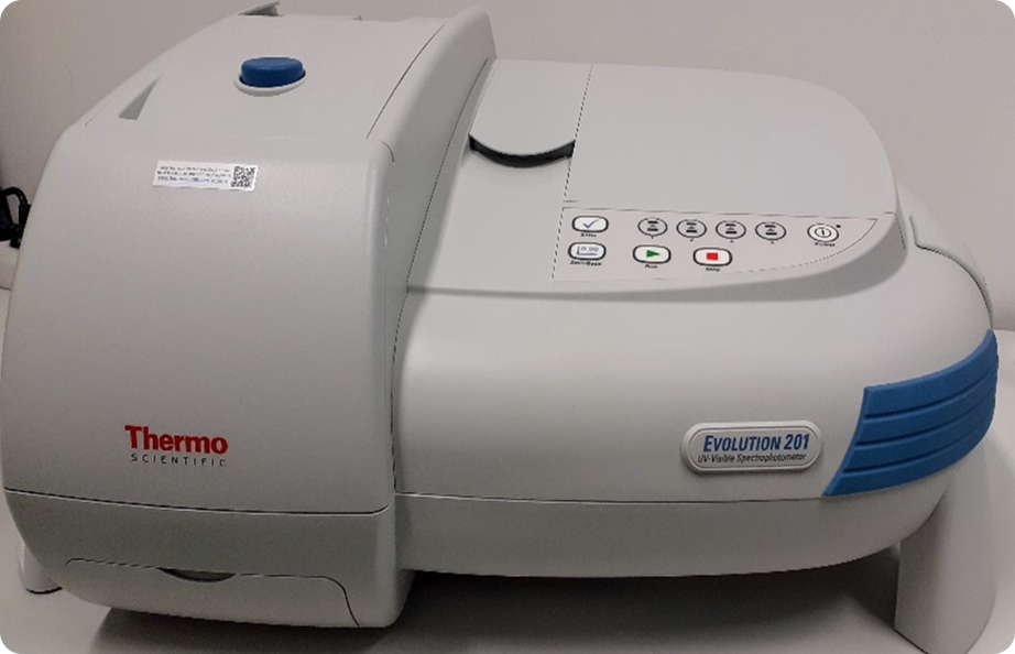
The device UV-Vis spectrophotometer EVOLUTION 201 has the following specifications:
- Spectrophotometer EVOLUTION 201: single beam spectrophotometer with Czerny-Turne monochromator
- Light source: halogen and deuterium lamp, detector: silicon photodiodes
- Measurement range: 200 - 1100 nm
- Scan mode: absorption, % transmittance, % reflection, Kubelka-Munk, log (1/R), log (Abs), Abs*factor, intensity
- Spectral bandwidth: 1 nm
- Scanning speed range: <1 to 6000 nm/min <1 to 6000 nm/min
- Contact:
- Assoc. Prof. Aleš Omerzu, PhD
- aomerzu@phy.uniri.hr
- +385 51 584 634
- Contact:
- Assoc. Prof. Aleš Omerzu, PhD
- aomerzu@phy.uniri.hr
- +385 51 584 634
Photoluminescence Spectrometer

How it works
Our device
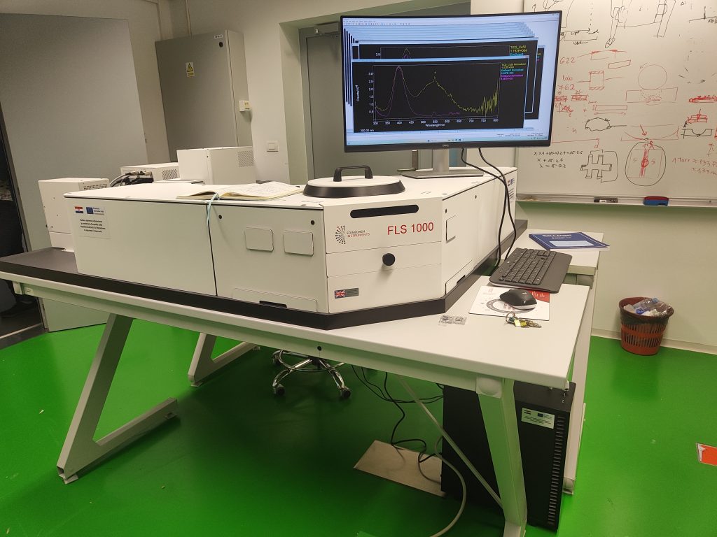
- Single-photon counting detector and associated electronics
- Instrument sensitivity: signal-to-noise ratio > 35,000:1 (measured on the Raman signal of water)
- Continuously tunable, computer-controlled bandpass
- Computer-controlled excitation and emission filter wheels for automated higher-order suppression, with 6 positions
- Monochromators: Double excitation monochromator, stray light suppression: > 1:10¹⁰, Single emission monochromator, stray light suppression: > 1:10⁵
- Light sources: CW Xe² lamp, 450 W, with integrated power supply, and pulsed μF² – 60 W
- Spectral range from 200 nm to 870 nm, with dark count rate < 50 cps and a response width of 600 ps <50 cps, te širinom odziva 600 ps
- Contact:
- Assoc. Prof. Ivna Kavre Piltaver, PhD
- ivna.kavre@uniri.hr
- +385 51 584 618
- Contact:
- Assoc. Prof. Ivna Kavre Piltaver, PhD
- ivna.kavre@uniri.hr
- +385 51 584 618
Cross-Section Polisher

How it works
Our device

Cross-Section Polisher IB-19530CP
- Cross-section polisher instrument that does not produce surface roughness, step artifacts, or contamination
- Fully automated operation, from vacuum generation and ion milling to fine milling and final polishing
- Milling speed up to 700 µm/h on silicon (at an accelerating voltage of 8 kV)
- Ion beam diameter of 500 µm
- Rotational holder enabling removal of stress layers generated by mechanical polishing, for samples of 40 mm (diameter) × 15 mm (V) or larger, with tilt capability from 0° to 90°
- One fixed argon ion gun (to avoid surface temperature increase and unwanted differential etching caused by multiple guns)
- Sample stage tilt angle of ±30° or greater to prevent curtain effects and redeposition
- Alternating (intermittent) milling with adjustable ON/OFF timer from 1 to 999 seconds or more, enabling maintenance of the sample surface temperature below 40 °C without the need for cryogenic cooling
- Capability for carbon coating using the argon ion gun within the cross-section polisher
- The CP system is capable of: Cross-section cutting, Flat surface polishing, Differential etching, Carbon coating of freshly cut samples inside the polisher
- Contact:
- Assoc. Prof. Ivna Kavre Piltaver, PhD
- ivna.kavre@uniri.hr
- +385 51 584 618
- Contact:
- Assoc. Prof. Ivna Kavre Piltaver, PhD
- ivna.kavre@uniri.hr
- +385 51 584 618
